The “Perfect Silicon Chip” Breakthrough That Could End Moore’s Law
Intermediate | March 4, 2026
✨ Read the article aloud on your own or repeat each paragraph after your tutor.
Moore’s Law Is Nearing the Finish Line
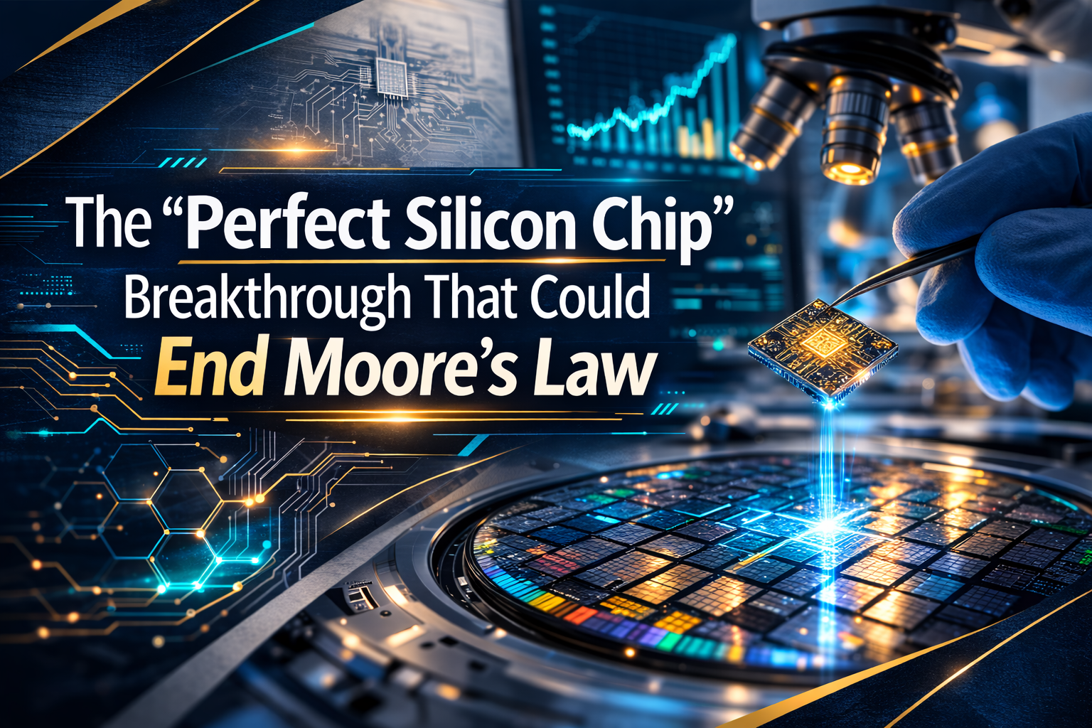
For decades, Moore’s Law has basically meant: chips keep getting smaller, faster, and cheaper because engineers can pack more transistors onto each new generation of silicon. But this perfect silicon chip innovation story suggests we’re getting close to silicon’s physical limit. But a recent report argues we may be approaching the final frontier—the smallest, most densely packed silicon chips that physics will allow. (WSJ)
The key bottleneck is photolithography, the “light-and-chemistry” process used to carve tiny patterns into silicon. Today’s most advanced patterning is already working at a crazy-small scale—measured in tens of atoms. (WSJ)
The Innovation: A New “Metal-Organic” Photoresist
So what’s the new idea? Researchers have been developing metal–organic frameworks (MOFs) and related “metal–organic” materials that can act as next-generation photoresists—the light-sensitive chemicals used in lithography. (WSJ)
Why does that matter? When chipmakers push to smaller sizes, the photoresist has to be extremely precise and stable. A big advantage of MOF-style materials is that they can be engineered to form very orderly nanoscale structures, which helps create cleaner, sharper patterns. (WSJ)
Going Beyond EUV: Using Shorter-Wavelength Light
Modern cutting-edge chips are made using EUV lithography (extreme ultraviolet) at a wavelength of 13.5 nm. But researchers are experimenting with something even shorter—soft X-ray / “beyond EUV” light around 6.5–6.7 nm. The shorter the wavelength, the smaller the features you can potentially print. (Tom’s Hardware)
A Johns Hopkins team described how soft X-ray approaches could boost resolution toward 5 nm and below, though they also admitted the industry is still years away from building full tools for this approach. (Tom’s Hardware)
Why This Is So Hard: It’s Not Just One Problem
Even if the chemistry works, the entire ecosystem is a massive challenge. Beyond-EUV would need breakthroughs in:
- Light sources powerful enough to be practical
- Mirrors/optics, because this kind of light is absorbed by many materials
- Resists that react correctly at these higher-energy wavelengths
- Masks and consumables to support mass production
That’s why some experts think this “last step” to reach the smallest possible silicon chips might not arrive commercially until around 2040. (WSJ)
The Business Angle: Why This Perfect Silicon Chip Innovation Could “End” Moore’s Law
Here’s the twist: this innovation could help engineers reach the end goal of Moore’s Law—meaning we finally achieve the “perfect” silicon chip density. After that, we won’t keep getting big gains just by shrinking features. Instead, progress may come more from packaging, stacking, and smarter system design (basically, building more powerful systems by combining chips in better ways).
So, the headline isn’t “technology stops.” It’s more like: with a perfect silicon chip innovation, we may reach the end of simple shrinking—then progress shifts to new strategies like packaging and stacking. It’s more like: the easy mode ends, and the next era becomes more expensive, more complex, and more about engineering trade-offs.
Vocabulary
- breakthrough (noun) – an important discovery or major success.
Example: The team’s breakthrough could push chipmaking to a new limit. - photolithography (noun) – using light to create tiny patterns on a material.
Example: Photolithography is how chip patterns get printed onto silicon. - photoresist (noun) – a light-sensitive chemical used in lithography.
Example: A new photoresist could make smaller, cleaner chip patterns. - precision (noun) – extreme accuracy.
Example: Chipmaking requires precision at the scale of atoms. - wavelength (noun) – the distance between waves of light.
Example: Shorter wavelength light can print smaller features. - extreme ultraviolet (EUV) (noun) – a type of light used for advanced lithography.
Example: EUV lithography is used in the most advanced chip factories today. - soft X-ray (noun) – higher-energy light with an even shorter wavelength.
Example: Soft X-ray methods could eventually go beyond EUV. - bottleneck (noun) – the main point that limits progress.
Example: Resist chemistry can become a bottleneck for smaller chips. - commercially viable (adjective phrase) – possible to use at scale for real business.
Example: A lab demo isn’t always commercially viable. - ecosystem (noun) – the network of tools, suppliers, and systems needed to make something work.
Example: Beyond-EUV needs a whole new manufacturing ecosystem.
Discussion Questions (About the Article)
- What problem is Moore’s Law running into as chips get smaller?
- What are MOFs, and why might they help chipmaking?
- Why does using a shorter wavelength light matter in lithography?
- Why might this technology take until around 2040 to become common?
- If shrinking chips slows down, what other methods might keep computing improving?
Discussion Questions (About the Topic)
- Do you think tech progress slows down when physics becomes the limit? Why or why not?
- Should governments subsidize advanced chip research, or should the market handle it?
- How would slower chip progress change smartphones, AI, or gaming?
- What industries would benefit most from “post-Moore’s Law” innovation?
- If you were a CEO, where would you invest: smaller transistors, better packaging, or new materials?
Related Idiom or Phrase
“Hit the ceiling” — to reach the highest possible limit.
Example: Silicon chipmaking may be hitting the ceiling, so engineers need new strategies.
📢 Want more practical English using real news? 👉 Sign up for the All About English Mastery Newsletter! Click here to join us!
Want to finally Master English but don’t have the time? Mastering English for Busy Professionals is the course for you! Check it out now!
Follow our YouTube Channel @All_About_English for more great insights and tips.
This article took inspiration from: ( WSJ ), ( Tom’s Hardware ), and Johns Hopkins University research listings on EUV/Beyond-EUV resist work ( Johns Hopkins University ).